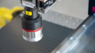
Precise to the micrometer
Integrating a solution for spot height testing
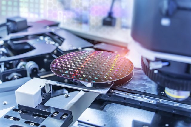
Electromobility is not only a major trend of our time but also a key driver for the development of new solutions and technologies. Both car manufacturers and their suppliers face new challenges. Innovative thinking is essential, but so is a commitment to quality: new components must consistently meet the highest standards. This is also true for our client, an internationally active specialist who manufactures monocrystalline silicon carbide semiconductor wafers used in electric vehicles, among other applications.
The challenge
Our client’s high-precision semiconductor wafers have a thickness of just 350 micrometers—about 0.3 millimeters. To ensure the consistently high quality of these semiconductors, reliable and accurate thickness inspection is crucial. However, this has been a significant challenge for the company. Conventional measuring methods often proved inaccurate and prone to errors, and were also time-consuming, impacting productivity.
The goal
In collaboration with our client, we defined the following objectives for our project:
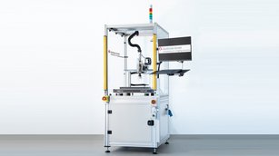
- Develop and integrate a test stand into the processes that allows precise measurement regardless of the test piece geometry.
- Ensure the new solution enables flexible measurement without requiring a fixed arrangement of the measuring positions.
- Reduce the measurement time while maintaining consistent accuracy.
To meet these criteria and develop a customized solution for our client, we conducted a comprehensive feasibility study in our specially equipped test laboratory.
The solution
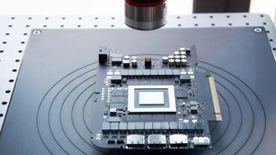
Our system—a stand-alone solution that performs both measurement and professional data analysis using its own software—is precisely tailored to our client's requirements. It reliably measures within predefined tolerance ranges for components with various geometries and enables flexible level measurement with positioning in all three spatial directions. Besides reducing reject rates, the system’s high speed and comprehensive analysis contribute to sustained improvements in the manufacturing process and a long-term increase in productivity.
This is why Goldlücke is the ideal partner
- 20 years of expertise in industrial image processing and the development of customized test systems and processes
- Comprehensive solutions from a single source, perfectly tailored to specific customer requirements
- Possibility to conduct feasibility studies in our in-house development laboratory
- Proprietary software to ensure reliable data analysis and continuous process optimization
- Highly qualified team with in-depth knowledge in mechanical and plant engineering, computer science, and electrical engineering
Do you have any questions about our systems?
Do you need a turnkey solution tailored to your requirements? We would be happy to discuss your needs and design a customized test system together. Feel free to send us a message or give us a call.